| Author |
 Topic Topic  |
|
|
chadbh74

USA
28 Posts |
 Posted - 12/12/2015 : 19:16:34 Posted - 12/12/2015 : 19:16:34


|
I'm trying to create a custom adapter board I can solder MBM29F033 (TSOP40) so that it will drop into the ZIF40 socket of the GQ-4X. I was able to determine most of the pin routing from the photo provided at the link here http://www.mcumall.com/forum/topic.asp?TOPIC_ID=6530
However, I'm unable to determine which ZIF pin the GQ-4X would use for the WE line. The GQ-USBProg software indicates to use a ADP-077 and ADP-082 board. This would be fine if I wasn't planning on taking the chip after it's soldered and putting it back into the GQ-4X later for reflashing. My custom PCB will take the TSOP40 layout of the 29F033 and adapt it to the 40 pin ZIF of the GQ-4X. If the pinout of the ZIF40 socket is correct when selecting the 29F033 then all I need is to know where to route the WE line. Anyone? |
- Chad H.
https://sites.google.com/site/cbhlab101 |
Edited by - chadbh74 on 12/13/2015 18:41:40
|
|
| Reply #1
anniel

2635 Posts |
Posted - 12/12/2015 : 19:53:08
|
| Which device definition will you use? |
 |
|
| Reply #2
chadbh74
USA
28 Posts |
Posted - 12/12/2015 : 21:04:24
|
This one provided in the devices.txt file
Name="MBM29F033C*TSOP40",ID="04D4",Class="29F040B",Category="FLASH",MFG="FUJITSU",CodeSize="4194304",DIP="100011110101",Adapter="TSOP40B-DIP32(ADP-077 and ADP-082)";
|
- Chad H.
https://sites.google.com/site/cbhlab101 |
|
|
| Reply #3
anniel
2635 Posts |
Posted - 12/13/2015 : 05:32:14
|
| DIP="100011110101" tells you pin 22. |
|
|
| Reply #4
chadbh74
USA
28 Posts |
Posted - 12/13/2015 : 06:58:58
|
| If its pin 22 for WE then the pinout in the above post link is wrong for this chip as it has Pin 22 being D4. I gues this is confirmed by the fact that a DIP32 adapter is being called for. I have been unable to find any information at all on these binary string configurations. Where can I find documentation to translate that string so I can determine the expected DIP32 pinout for this chip? Thanks! |
- Chad H.
https://sites.google.com/site/cbhlab101 |
Edited by - chadbh74 on 12/13/2015 07:01:11 |
|
|
| Reply #5
anniel
2635 Posts |
Posted - 12/13/2015 : 07:42:12
|
| Bit #8 : ZIF pin 22 mapped to CE(WE) when it is '1'. Otherwise the ZIF pin 22 will be logic '0' always. |
|
|
| Reply #6
chadbh74
USA
28 Posts |
Posted - 12/13/2015 : 09:50:08
|
| Where is a table on what each of the bits do? Also, that just identifies pin 22, I still need to know what the other 31 pins of the DIP32 adapter are mapped to at the ZIF adapter since the standard 40 pinout is apparently invalid with the adapter. |
- Chad H.
https://sites.google.com/site/cbhlab101 |
Edited by - chadbh74 on 12/13/2015 09:55:54 |
|
|
| Reply #7
anniel
2635 Posts |
Posted - 12/13/2015 : 10:45:07
|
In your original post you state you have found the other pins.
You can trace the official adapter to find the mapping or you can use the datasheets to make you own.
Bit #1 : ZIF pin 16 GND control. When it is '1', the pin 16 of ZIF is GND signal. '0' is GND off.
Bit #2 : ZIF pin 1 mapped to A19 when it is '1'. When this bit is '1', Bit#3 must be '0'
Bit #3 : ZIF pin 1 mapped to A18 when it is '1'. When this bit is '1', Bit#2 must be '0'
Bit #4 : ZIF pin 29 mapped to CE when it is '1'. When this bit is '1', Bit#5 must be '0'
Bit #5 : ZIF pin 29 mapped to A14 when it is '1'. When this bit is '1', Bit#4 must be '0'
Bit #6 : ZIF pin 24 mapped to OE when it is '1'. Otherwise the ZIF pin 24 will be logic '0' always.
Bit #7 : ZIF pin 28 mapped to A13 when it is '1'. Otherwise the ZIF pin 28 will be logic '0' always.
Bit #8 : ZIF pin 22 mapped to CE(WE) when it is '1'. Otherwise the ZIF pin 22 will be logic '0' always.
Bit #9 : ZIF pin 30 mapped to A13 when it is '1'. Otherwise the ZIF pin 30 will be logic '0' always.
Bit #10: ZIF pin 30 mapped to A17 when it is '1'. Otherwise the ZIF pin 30 will be logic '0' always.
Bit #11: ZIF pin 31 mapped to CE(WE) when it is '1'. When this bit is '1', Bit#12 must be '0'
Bit #12: ZIF pin 31 mapped to A18 when it is '1'.When this bit is '1', Bit#11 must be '0'
|
|
|
| Reply #8
anniel
2635 Posts |
Posted - 12/13/2015 : 11:10:08
|
| What standard 40 pinout? |
|
|
| Reply #9
chadbh74
USA
28 Posts |
|
| Reply #10
chadbh74
USA
28 Posts |
Posted - 12/13/2015 : 13:06:33
|
My best guess right now, and this is just a guess...
The chip profile, even though it is a TSOP40, is using the 29F040B class, which is a DIP32 chip. Sooo.. if I take the 29F040B pinout from its data sheet and apply the bit changes then I should have the pinout?
If this were true, that still leaves the A19, A20, A21 to figure out. These don't exist in a 29F040B. |
- Chad H.
https://sites.google.com/site/cbhlab101 |
Edited by - chadbh74 on 12/13/2015 13:47:46 |
|
|
| Reply #11
anniel
2635 Posts |
Posted - 12/13/2015 : 14:10:18
|
You realize the pinout of your link is for the GQ ZIF, not for a particular chip or adapter, do you?
Yes it uses the 29F040B class, you are correct. You also have to keep in mind that the adapter has some logic and other components on it.
A19, A20 and A21 are already figured out in your link as all the other signals you need. |
|
|
| Reply #12
chadbh74
USA
28 Posts |
Posted - 12/13/2015 : 16:06:54
|
| Yes, I saw the chips on board, but without a pinout to the ZIF and without a schematic and without the adapter itself it's all a mystery. Either I will have to purchase the adapters, which is expensive and still doesn't guarantee success, or pursue this concept based upon the interface of another device programmer |
- Chad H.
https://sites.google.com/site/cbhlab101 |
|
|
| Reply #13
anniel
2635 Posts |
Posted - 12/13/2015 : 16:24:34
|
???
Which adapter is expensive?
Why wouldn't it work with the official adapter?
If you use the pinout of the link and match it to the pinout of the datasheet, it doesn't work? |
|
|
| Reply #14
chadbh74
USA
28 Posts |
Posted - 12/13/2015 : 16:52:20
|
I'm sure the official adapter does work, but I don't have one. Even If I did, which would require atleast 2 adapters mated together, the ADP-082 and ADP-077, that contraption would only work for a unsoldered chip. I want to make a SINGLE compact PCB that I can solder the 29F033 to and drop that right into the GQ-4X for programming. If there existed a DIP version of this chip I would obviously save myself the trouble and go for that but I can't find one.
Here is a photo of something very similiar. I want to make this kind of board to attach the 29F033 to, drop it in the GQ-4X..simple.
www.buyicnow.com/bp.php?i=2586 |
- Chad H.
https://sites.google.com/site/cbhlab101 |
Edited by - chadbh74 on 12/13/2015 16:53:42 |
|
|
| Reply #15
anniel
2635 Posts |
Posted - 12/13/2015 : 17:04:21
|
| Yes, I understand, but what doesn't work when you try? |
|
|
| Reply #16
anniel
2635 Posts |
Posted - 12/13/2015 : 17:06:09
|
| It seems to be a simple adapter to make. |
|
|
| Reply #17
chadbh74
USA
28 Posts |
Posted - 12/13/2015 : 17:17:57
|
| Try what? I can't try anything because I don't have the adapter and I don't have the pinout information and I don't have any schematics to shed light on this. |
- Chad H.
https://sites.google.com/site/cbhlab101 |
|
|
| Reply #18
chadbh74
USA
28 Posts |
Posted - 12/13/2015 : 17:25:57
|
I found on another McuMall forum post that the ADP-082 utilizes a 74HC244 line driver. This must be how it's sending the signals for the extra address lines.
I also found another post with this image here for the ADP-082 header. I'm not quiet sure it is complete or shows the information I would need to make a board to attach to the ADP-082. The 29F033 calls for a TSOP40B configuration.
Image Insert:
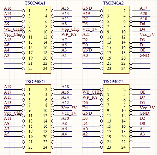
143.55�KB |
- Chad H.
https://sites.google.com/site/cbhlab101 |
Edited by - chadbh74 on 12/13/2015 17:26:19 |
|
|
| Reply #19
anniel
2635 Posts |
Posted - 12/13/2015 : 19:54:38
|
What extra address lines? The MBM29F033 only has 22 address lines.
What pinout information you don't have? Are you missing the MBM29F033 datasheet?
If you use the pinout of the link and match it to the pinout of the datasheet, it doesn't work?
I don't understand what you are needing more.
If you absolutely need a schematic just take a pencil and draw it! |
|
|
| Reply #20
chadbh74
USA
28 Posts |
Posted - 12/14/2015 : 05:51:06
|
| Like I've been saying the whole time... the bottom DIP32 pinout used by the ADP-082 adapter, not the top headers as in the photo I pasted. |
- Chad H.
https://sites.google.com/site/cbhlab101 |
|
|
| Reply #21
anniel
2635 Posts |
Posted - 12/14/2015 : 06:05:04
|
The bottom of ADP-082 adapter is not DIP32, where did you get that?
The ADP-082 adapter top headers pinout is irrelevant since you want to make you own DIP to TSOP adapter.
Simply follow the pinout below with the MBM29F033 datasheet in hand.
 |
|
|
| Reply #22
chadbh74
USA
28 Posts |
Posted - 12/14/2015 : 10:16:07
|
From the adapter string...
Name="MBM29F033C*TSOP40",ID="04D4",Class="29F040B",Category="FLASH",MFG="FUJITSU",CodeSize="4194304",DIP="100011110101",Adapter="TSOP40B-DIP32(ADP-077 and ADP-082)";
Not only is the adapter being referred to as DIP32 but the 29F040B class chip is also a DIP32
Also, that ZIF40 image has no indication of where the WE line is at. You say the bin string put it at pin 22, but then where would the D4 be at? |
- Chad H.
https://sites.google.com/site/cbhlab101 |
Edited by - chadbh74 on 12/14/2015 10:55:50 |
|
|
| Reply #23
anniel
2635 Posts |
Posted - 12/14/2015 : 11:03:37
|
Ha now I understand your confusion.
The device string is kept at a minimum requirement to maintain backward compatibility with the GQ-3X and previous models for the software.
The actual ADP-082 adapter has 36 pins not 32, if you use an older programmer you need to snip off 4 pins and use an extra header.
The DIP setting is also based on 32 pins for the same reason, calculate where pin 22 is at based on a DIP 32 and you'll understand.
The device string is of no interest to build an adapter, except if the DIP setting has pin fonctions switched.
Simply follow the pinout of my previous post with the MBM29F033 datasheet and you are all set.
|
Edited by - anniel on 12/14/2015 11:08:31 |
|
|
| Reply #24
chadbh74
USA
28 Posts |
Posted - 12/14/2015 : 16:32:11
|
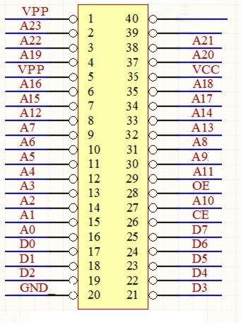
36 instead of 32 pins..That explains where the extra address lines are routed. But that's not the only source of confusion. The ZIF40 image above does NOT show a WE line. I believe there are 2 errors on that pinout.
I took the following pinout for the M29F040B DIP32, as this is the class chip being specified in the configuration...
Image Insert:
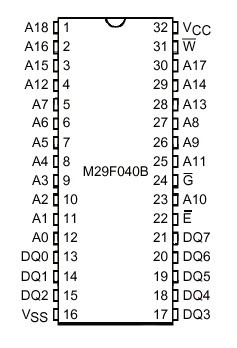
25.06�KB
Then I used it to make the 2 corrections to the original ZIF40 pinout image ...
Image Insert:
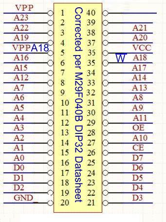
42.69�KB![]()
If this is in fact the actual pinout for the ZIF40, then I could make a DIP36 adapter and shorten the configuration for the 29F033 to something like this ...
Name="MBM29F033C*DIP36",ID="04D4",Class="29F040B",Category="FLASH",MFG="FUJITSU",CodeSize="4194304",Adapter="Custom"
Is this about right? |
- Chad H.
https://sites.google.com/site/cbhlab101 |
Edited by - chadbh74 on 12/14/2015 16:37:44 |
|
|
| Reply #25
chadbh74
USA
28 Posts |
Posted - 12/14/2015 : 16:51:19
|
I believe stating that the ZIF40 pinout is always the same is misleading. Surely it depends on the CLASS of chip in the configuration string.
Take the common 27512 DIP28...
Image Insert:
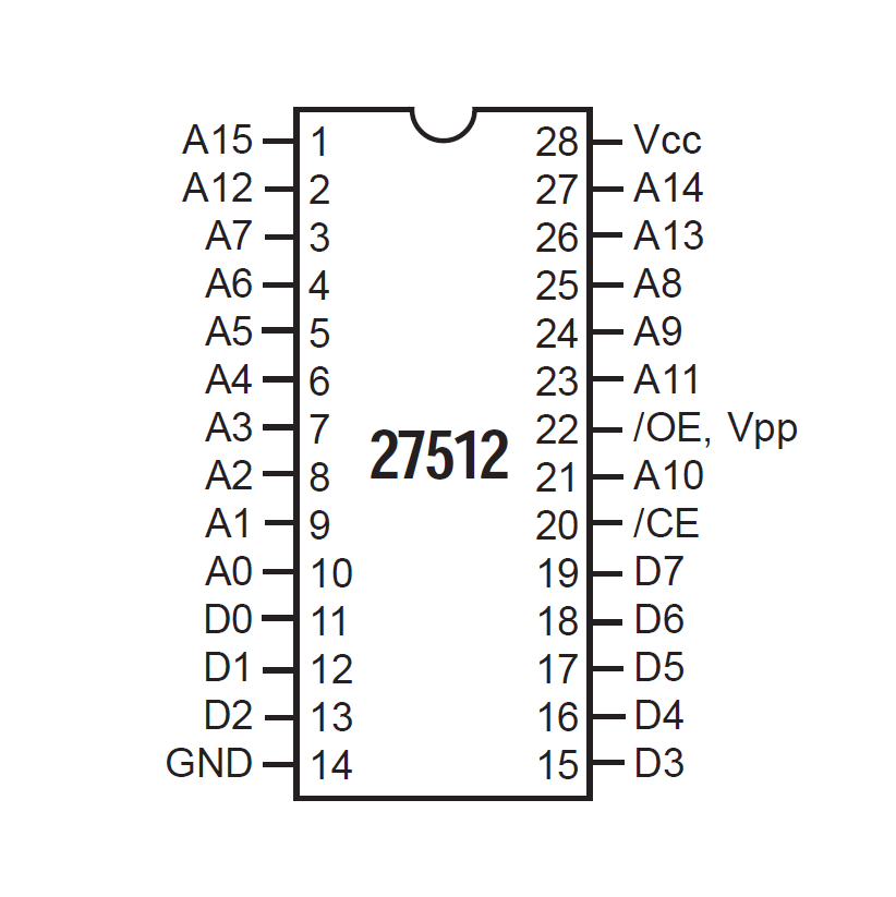
53.42�KB
At pin 34 of the ZIF40, it replaces A17 with VCC. As a person new to the GQ-4X, I found the ZIF40 pinout as originally posted by ZLM on another post and took it to mean that its that way all the time. This of course isn't 100% true since different chips, even those DIP chips that drop right into the programmer, have different pinouts.
So we need to go by the pinout of the chip referenced to by the CLASS in the configuration correct? |
- Chad H.
https://sites.google.com/site/cbhlab101 |
Edited by - chadbh74 on 12/14/2015 16:57:53 |
|
|
| Reply #26
anniel
2635 Posts |
Posted - 12/14/2015 : 17:18:59
|
Could be errors, I am not the original poster nor creator of the pinout.
ZLM http://www.mcumall.com/forum/pop_profile.asp?mode=display&id=134 is and he should correct it in his files since he seems to be the official MCU Mall help department.
Name="MBM29F033C*DIP36" should be Name="MBM29F033C*TSOP40" rest should be ok. |
|
|
| Reply #27
anniel
2635 Posts |
Posted - 12/14/2015 : 17:27:50
|
I also assumed it to be the case as stated by ZLM.
I suppose you are right, the CLASS could also change the pinout. |
|
|
| Reply #28
chadbh74
USA
28 Posts |
Posted - 12/14/2015 : 17:29:14
|
He probably intended it to be the pinout for some very large 40-pin chip that had A0-A23 address lines. Assuming that was a fixed configuration for all chips supported by the GQ-4X was naive on my part I guess.
The only other question in my mind is the resistors utilized on the ADP-082 adapter. Was there any purpose for them other than voltage control for some 3V chips?
I'm guessing, since the 29F033 is a 5V only chip, I shouldn't need any resistors or regulation. It should take it just like the MB29F040B which is also 5V. |
- Chad H.
https://sites.google.com/site/cbhlab101 |
|
|
| Reply #29
anniel
2635 Posts |
Posted - 12/14/2015 : 17:33:55
|
I also didn't give it reflexion.
The different voltages can also be set from the device string. |
|
|
| Reply #30
chadbh74
USA
28 Posts |
Posted - 12/14/2015 : 17:34:58
|
| I think I have enough information now to begin working on my schematic. I will post the results of this indeavor here for future reference. Thank you for your help! |
- Chad H.
https://sites.google.com/site/cbhlab101 |
Edited by - chadbh74 on 12/14/2015 17:36:24 |
|
|
| Reply #31
anniel
2635 Posts |
|
| Reply #32
ZLM

2949 Posts |
Posted - 12/14/2015 : 20:55:20
|
The ZIF pin out is configurable. It is depending on how you define the device line DIP= keyword.
example:
for 29F040 used DIP = 101011100110
for 27C512 used DIP = 100010110000
It represents a standard traditional Willem programmer DIP switch.
Image Insert:
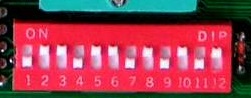
12.39�KB
There are 12 bits total from left to right start from Bit #1
Bit #1 : ZIF pin 16 GND control. When it is '1', the pin 16 of ZIF is GND signal. '0' is GND off.
Bit #2 : ZIF pin 1 mapped to A19 when it is '1'. When this bit is '1', Bit#3 must be '0'
Bit #3 : ZIF pin 1 mapped to A18 when it is '1'. When this bit is '1', Bit#2 must be '0'
Bit #4 : ZIF pin 29 mapped to CE when it is '1'. When this bit is '1', Bit#5 must be '0'
Bit #5 : ZIF pin 29 mapped to A14 when it is '1'. When this bit is '1', Bit#4 must be '0'
Bit #6 : ZIF pin 24 mapped to OE when it is '1'. Otherwise the ZIF pin 24 will be logic '0' always.
Bit #7 : ZIF pin 28 mapped to A13 when it is '1'. Otherwise the ZIF pin 28 will be logic '0' always.
Bit #8 : ZIF pin 22 mapped to CE(WE) when it is '1'. Otherwise the ZIF pin 22 will be logic '0' always.
Bit #9 : ZIF pin 30 mapped to A13 when it is '1'. Otherwise the ZIF pin 30 will be logic '0' always.
Bit #10: ZIF pin 30 mapped to A17 when it is '1'. Otherwise the ZIF pin 30 will be logic '0' always.
Bit #11: ZIF pin 31 mapped to CE(WE) when it is '1'. When this bit is '1', Bit#12 must be '0'
Bit #12: ZIF pin 31 mapped to A18 when it is '1'.When this bit is '1', Bit#11 must be '0'
Those pin numbers are referring to a 32 pin ZIF socket.
For 40 pin ZIF socket, the top 8 pins are fixed. So, only lower 32 ZIF pins can be reconfigured and mapped to a traditional 32 pin Willem programmer.
|
|
|
| Reply #33
anniel
2635 Posts |
Posted - 12/15/2015 : 03:19:46
|
Yes I know about the DIP settings.
How do you explain both a 27512 and a M29F040B have no DIP in the devices.txt but they have different pinouts?
Does the Class keyword in the devices.txt gives a starting point for the pinout of the ZIF fixed in the software? |
|
|
| Reply #34
ZLM
2949 Posts |
Posted - 12/15/2015 : 12:37:10
|
Each Class has an internal default DIP setting. The DIP= setting in device line is to overwrite the default.
As long as you selected a Class, the default DIP setting for that class will be used. |
|
|
| Reply #35
anniel
2635 Posts |
Posted - 12/15/2015 : 13:23:41
|
| OK that explains it all. Thank you for the clarification. |
|
|
| Reply #36
chadbh74
USA
28 Posts |
Posted - 12/15/2015 : 20:39:17
|
| Yes ZLM, thanks for the info. I've ordered a sample test batch of the custom TSOP40 - DIP36 adapter I made based off of the updated pinout chart above (M29F040B). The only other components I included on the adapter was a 0.1uf capacitor for power stability. It may not be needed but it can't hurt. I will test the board with and without to see if there is a difference |
- Chad H.
https://sites.google.com/site/cbhlab101 |
|
|
| Reply #37
anniel
2635 Posts |
Posted - 12/17/2015 : 09:31:57
|
| @chadbh74 Keep us informed. |
|
|
| Reply #38
chadbh74
USA
28 Posts |
|
| Reply #39
chadbh74
USA
28 Posts |
Posted - 01/09/2016 : 12:02:30
|
Well I've been testing the prototype PCB's and they are working flawlessly based off of the 29F040B pinout mapping combined with mapping of the extra address pins at the top of the ZIF-40. So a DIP-36 configuration was sufficient to map the TSOP 40 chip fully. There were specialized pins on the TSOP40 pinout that are not used by the GQ-4X. Also, no capacitor was required on the power rails. I tried once and it seemed to interrupt the process so I removed the capacitor.
Since I followed the standard 29F040B layout I could eliminate the DIP setting and I added the following chip profile...
Name="MBM29F033C*DIP36",ID="04D4",Class="29F040B",Category="FLASH",MFG="FUJITSU",CodeSize="4194304",Adapter="Custom";
I could not keep the *TSOP40 at the end of the Name or it would conflict with the existing entry...there MUST be a difference for them to list properly.
Thanks for the help everyone, hope this helps others with projects like this. Now all I have to do is design my device based around the pinout of my board and use the GQ-4X to (re)program it.. Simple :)
Download Attachment: 
5493309
Image Insert:
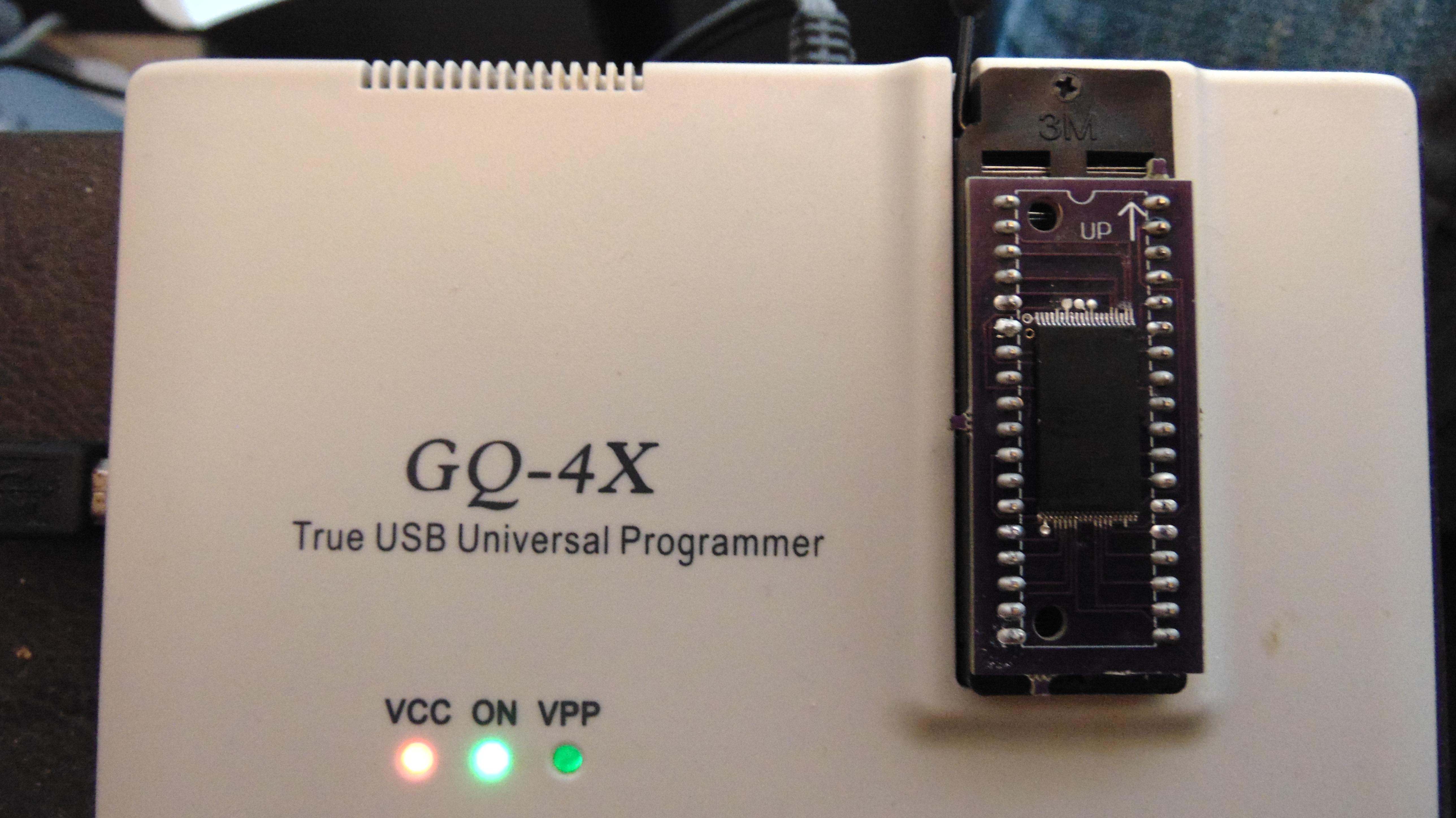
1149401 bytes![]() |
- Chad H.
https://sites.google.com/site/cbhlab101 |
Edited by - chadbh74 on 01/10/2016 12:31:29 |
|
|
| Reply #40
anniel
2635 Posts |
Posted - 01/10/2016 : 04:44:45
|
| Nice hack. Why the two big holes in the board? |
|
|
| Reply #41
chadbh74
USA
28 Posts |
|
| Reply #42
anniel
2635 Posts |
Posted - 01/10/2016 : 14:41:47
|
| OK :) |
|
|
| |
Topic |
|
